Hello everyone, Welcome to Electrical Maker, Today We will Discuss an interesting Topic on How the MOSFET Works. Electrical Maker provides all important information about this topic.
Contents
What is a MOSFET?
In this article, we will understand the basics concept of MOSFET and we will also understand how the MOSFET works.
MOSFET stands for metal oxide semiconductor field-effect transistor which is the combination of field-effect concept and MOS technology.
MOSFET or MOS-FET is a type of transistor used for amplifying or switching electronics signals in electronic devices.
It is a core of an Integrated circuit and it can be designed and fabricated in a single chip because of these very small sizes.
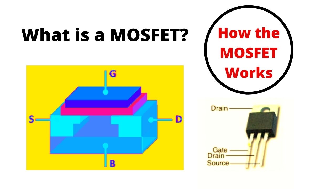
The MOSFET is a four-terminal semiconductor device. The four terminals of the MOSFET are gate, drain-source, and body.
The body of the MOSFET is frequently connected to the source terminal so making it a 3 terminal device like FET(field effect transistor).
It is a majority carrier device and in the case of majority carriers there is not any recombination delay hence it achieves extremely high bandwidth and switching time.
It does not have a 2ndry breakdown area, its drain to source resistance has a positive temperature coefficient, so it tends to be self-protective.
When in forward biased, it has very low ON resistance and no junction voltage drop.
Due to the above features, MOSFET is an extremely attractive power supply switching device. It is also called IGFET (Insulated Gate FET).
MOSFET is the most common transistor and can be used in both digital and analog circuits.
MOSFET Full Form
MOSFET stands for metal oxide semiconductor field-effect transistor
Symbol for Mosfet
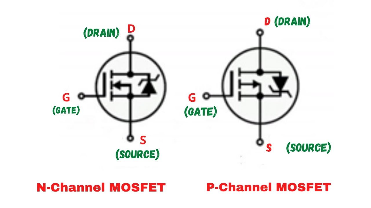
Types of MOSFET
MOSFET is basically of two types one is Depletion enhancement type MOSFET (DEMOS) and another is Enhancement only MOSFET (E-ONLY MOS).
Depletion type and Enhancement type is further classified into N- channel and P- channel like
|
|
|
|
Depletion –Enhancement MOSFET (DEMOS)
This MOSFET is named the depletion enhancement MOSFET because it can be operated in both the depletion mode as well as the enhancement mode by changing the polarity of the gate to source voltage (VGS).
When a negative gate to source voltage (VGS) is applied then the n-channel DE-MOSFET operates in the depletion mode.
However when a positive gate to source voltage is applied then it operates in the enhancement mode.
As a channel exists between drain and source, then a drain current (ID) flows even when VGS= 0. Due to this reason, DE-MOSFET is known as ON-MOSFET.
Enhancement – only MOSFET (E-ONLY MOS)
As the name indicates, this MOSFET can be operated only in the enhancement mode and not in depletion mode. This MOSFET work with the large positive gate to source voltage only.
It differs from the DE-MOSFET in construction as DE-MOSFET has a channel between drain and source whereas this E-only MOSFET does not have any channel between drain and source.
As this MOSFET does not have any channel so it does not conduct when VGS = 0. That is why this MOSFET is called OFF MOSFET.
In the case of DEMOS, ID flows even when the gate to source voltage is zero. It operates in depletion mode with a negative value of VGS. As VGS is made more negative, ID decreases till it ceases when VGS= VGS(Off) = VT(Threshold).
It works in enhancement mode when VGS is positive.
In the case of E-only MOSFET, drain current ‘ID’ flows only when VGS exceeds VT.
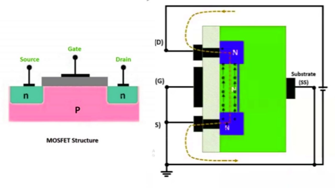
Construction of MOSFET
Here we will understand the construction of MOSFET by taking an example of DE-MOSFET.
A MOSFET has a source, gate, and drain just like JFET. The gate of the Mosfet is insulated from its conducting channel by a very thin insulating film of metal- oxide usually of silicon dioxide Sio2. Due to this insulating property, MOSFET is also known as an insulated-gate field-effect transistor (IGFET).
In this, the drain current is controlled by the gate voltage just like JFET but the main difference between JFET and MOSFET is that in the latter case we can apply a positive and negative voltage to the gate because it is insulated from the channel.
However, the gate, SiO2 insulator, and channel form a parallel plate capacitor. Unlike junction field-effect transistor a DEMOSFET has only one P- region or N-region called the substrate. Normally the substrate is shorted to the source internally.
How The MOSFET Works
The working of a MOSFET can be explained in two modes one is depletion mode and another is enhancement mode.
(a)Depletion Mode of N-channel DEMOSFET
When VGS = 0
In this case, electrons can flow freely from source to drain through the conducting channel that exists between drain and source.
When a negative voltage is applied to the gate then it depletes the N-channel of its electrons by including a positive charge in it.
AS the greater the negative voltage applied in the gate, the greater will be the reduction in the number of electrons in the channel and consequently lesser is its conductivity.
In fact, too much negative gate voltage called VGS (off) = VT can off the Channel. For this clear reason, the negative gate operation of a DE-MOS is called its depletion mode operation.
(b) Enhancement Mode of N channel DEMOSFET
In this mode of operation again drain current (ID) flows from source to drain even when a gate bias voltage is zero.
When a positive voltage is applied to the gate then the input gate capacitor is able to create free electrons in the channel which increases the drain current (ID).
When the positive gate voltage is increased then the number of induced electrons is increased as a result the conductivity of the source to drain channel is increased and accordingly increasing the number of current flows between the terminals.
Due to this reason, the positive gate operation of a DE-MOSFET is known as enhancement mode operation.
| S.NO | Mode of Operation | Working of N- Channel MOSFET as |
| 1. | Active Region | Amplifier |
| 2. | Cut off Region | Open Switch |
| 3. | Saturation Region | Closed Switch |
Advantages of MOSFET
- It can be made quite small in size and it occupies a very small area on the silicon Integrated chip.
- The manufacturing of MOSFET is quite simple.
- MOSFET is greatly used as compared to BJT and JFET in its application in VLSI.
- It is used in microprocessors, memory chips, analog ICs as well as IC using both analog and digital ICs.
- It provides greater efficiency even when operating at lower voltages.
- The absence of gate current creates more input impedance which provides increased switching speed of the device.
- It can operate at a minimal power level and uses minimal current.
- The digital logic and the memory function can be enforced with the circuits using only the MOSFET and no diode or resistor is needed.
Disadvantages of MOSFET
- Instability of the devices when it is operated at overload voltage level.
- As there is a thin silicon oxide layer is present in the MOSFET it may create damage to the device when encouraged by the electrostatic charges.
Application of MOSFET
- MOSFETs are used in input amplifiers in oscilloscopes and electronic voltmeters.
- It is used as voltage variable resistors in computer memories.
- MOSFETs are used in logic circuits, for mixing operation of FM in TV receivers.
- It provides regulation for DC motor.
- Since MOSFETs have enhanced switching speeds so it is used for the construction of chopper amplifiers.
I hope You like this Article On How the Mosfet Works. For any doubt and suggestions comment below.

Jitu Kumar is the Founder and Senior Content Head of Electrical Maker. On electricalmaker.com, we publish the latest educational updates regarding Engineering.